展会邀请 | 会议议程来了!半导体封装测试暨玻璃基板生态展 (CSPT*iTGV 2026)

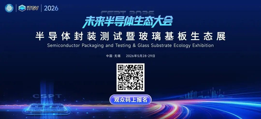
半导体封装测试暨玻璃基板生态展
? 无锡国际会议中心(江苏省无锡市滨湖区清舒道100号)? 太湖D厅 / 102A / 102C / 105DAY 15月27日 星期三 · 专题论坛 Wed. May 27专题论坛一 2.5D/3D IC 集成与封装大会
2.5D/3D IC Integration and Packaging Conference专题论坛二架构之光 - IC 设计论坛
Architecture Spotlight - IC Design专题论坛三短期培训课程
Short-term Training CourseDAY 25月28日 星期四 · 主论坛 & 专题论坛 Thur. May 28主论坛一未来半导体生态大会暨 CSPT Awards 2026 颁奖
Future Semiconductor Ecosystem Conference & CSPT Awards 2026⏰ 08:30-12:10 ? 无锡国际会议中心 太湖D厅徐冬梅 中国半导体行业协会副秘书长兼封装分会秘书长卓胜微射频前端技术演进与未来生态布局Maxscend's RF Front-End Technology Evolution and Future Ecological Layout冯晨晖 江苏卓胜微电子股份有限公司 创始人之一、副总经理2.5D 异构集成封装技术发展趋势Development Trends in 2.5D Heterogeneous Integration Packaging Technology下一代 GPU 芯片组的趋势、挑战与产业链机遇Trends, Challenges, and Supply Chain Opportunities for Next-Generation GPU Chipsets硅芯科技成果发布:AI+2.5D/3D 3Sheng Integration Platform光电融合对中国半导体生态的发展要求Development Requirements for China's Semiconductor Ecosystem in the Context of Optoelectronic Integration应用于先进封装的多维度仿真分析以及芯德科技封装解决方案Multidimensional Simulation Analysis for Advanced Packaging & Turnkey Packaging Solutions from JSSI封装定义智能体:从汽车到机器人的芯片集成革命与生态共赢Packaging-Defined Agents: The Chip Integration Revolution from Automotive to Robotics and the Path to Ecosystem Synergy李太龙 江苏长电科技股份有限公司 智能驾驶与信息娱乐业务负责人从芯片失效分析看AI大潮下的半导体发展趋势Semiconductor Development Trends in the AI Era: Insights from Chip Failure AnalysisDAY 25月28日 星期四 · 主论坛 & 专题论坛 Thur. May 28主论坛二中国半导体封装测试技术与市场大会(CSPT 2026)
China Semiconductor Packaging Test Technology and Market Conference⏰ 13:30-18:10 ? 无锡国际会议中心 太湖D厅主持人于宗光 中国电子科技集团公司第五十八研究所 首席科学家Multi-physics Simulation of Advanced Packaging Empowers AI to Meet Future Challenges面对AI时代的先进封装Advanced Packaging for the AI Era 面向算力/射频/光电等多种应用的键合技术及原理Bonding Technologies and Mechanisms for Computing, RF, and Optoelectronic Applications刘子玉 恩纳基智能装备(无锡)股份有限公司 首席科学家协同创新 , 驱动未来:先进封装减薄与切割工艺链的深度融合Collaborative Innovation, Driving the Future: Deep Integration of Advanced Packaging Grinding and Laser Cutting Process Chains用于先进封装芯片的全自动无损检测的3D X 射线检测技术Fully Automatic Non-destructive 3D X-ray Technology for Advance Package IC
唐立云 康姆艾德机械设备 ( 上海 ) 有限公司中国技术销售总监
人工智能时代下的先进封装设计与分析Advanced Packaging Design and Analysis in the Age of Artificial Intelligence先进封装 - PVD 解决方案PVD Solutions For Advanced Packaging先进封装设备赋能异构集成新生态Advanced Packaging Equipment Empowers a New Ecosystem of Heterogeneous Integration余飞 北京北方华创微电子装备有限公司 市场产品解决方案总监 何洪文 华进半导体封装先导技术研发中心有限公司 代理 CEO先进封装关键装备及核心技术突破Key Equipment and Core Technology Breakthroughs in Advanced Packaging力森诺科集团在先进封装材料领域的研发策略及成果RESONAC's R&D strategy and advanced semiconductor packaging materials后摩尔时代,封测为王 - 中国半导体的突围之路In the Post-Moore Era, Packaging & Testing Takes the Lead - The Breakthrough Path of China's Semiconductor IndustryPeter Lee 中芯国际集成电路制造有限公司 投资经理人工智能时代功率半导体技术创新与挑战Power Semiconductor Technology Innovation and Challenges in the Age of Artificial Intelligence刘国友 株洲中车时代电气股份有限公司 首席技术专家专题论坛五3D IC 与先进封装材料创新合作大会
3D IC and Advanced Packaging Materials Innovation Cooperation Conference高性能环氧塑封料:驱动先进封装的关键材料High-Performance Epoxy Molding Compound: The Key Material Driving Advanced Packaging刘红杰 江苏华海诚科新材料股份有限公司研发 副部长杭州之江半导体先进封装材料解决方案Hangzhou Zhijiang Advanced Packaging Material Solutions for Semiconductors蓝宝石载盘在先进封装中的应用Applications of Sapphire Carriers in Advanced Packaging从智能化到 AI 化:先进封测工厂的智造进阶与 A 应用From Intelligence to AI Empowerment: Intelligent Upgrading and AI Application of Advanced Packaging and Testing FactoriesApplication and Analysis of Vertical Dynamic Storage & Retrieval Systems in the Roger Shi 卡迪斯物流设备(北京)有限公司大中华区及日本销售总监High-Reliability Metal TIM Solutions for Advanced PackagingRecent Technological Advances in Packaging Substrate Materials for the Era of High-Performance AI Computing
麦德美爱法针对 AI 数据中心应用的整体解决方案MacDermid Alpha Integrated Solutions for AI Data Center代 鹏 确信爱法金属(上海)贸易有限公司 战略市场经理超低温固化光敏聚酰亚胺(PSPI)在先进封装中的应用与技术突破Application and Technological Breakthrough of Ultra-Low Temperature Curing Photosensitive Polyimide (PSPI) in Advanced Packaging高可靠性BCB材料赋能先进封装 - 面向高密度异构集成的解决方案High-reliability BCB materials empower advanced packaging - A solution for high-density heterogeneous integrationAI 应用驱动下ABF载板技术需求演变Evolution for ABF Substrates for AI Application专题论坛六5月28日「AI 破局·芯生态」2026 无锡IC设计协同创新论坛
"AI Breakthrough - Chip Ecosystem" 2026 Wuxi IC Design Collaborative Innovation Forum从对话到执行:Agentic AI 驱动计算范式大迁徙From Dialogue to Execution: The Great Computing Paradigm Migration Driven byAgentic AI希姆计算,推动 RISC-V AI 算力跨越Stream Computing,Driving RISC-V AI Computing Power to New Heights端侧算力进化论:从生成式 AI 到机器人的物理智能地瓜机器人
Evolution of Multi-Scale High-Performance Interconnect Technology面向边缘AI的GPU IP架构演进与生态创新GPU Architecture Evolution and Ecosystem Innovation for the Edge AI EraAI for Chip 初探A Preliminary Exploration of AI for Chip倪潇飞 时擎智能科技(上海)有限公司 SoC研发高级经理芯连AI未来 - 牛芯赋能AI时代高速互联新生态Chip-Connected AI Future - KNiulink Empowering the New High-Speed Interconnect Ecosystem in the AI Era邬红缨 牛芯半导体(深圳)股份有限公司 市场副总经理MLCC如何为AI服务器与智能汽车"保电压、稳算力"?专题活动先进封装圈层交流暨中国玻璃线路板产业联盟筹备座谈会
Advanced Packaging Community Exchange & Preparatory Symposium of the China Glass Circuit Board Industry Alliance主题分享二:各环节关键挑战与突破点(拟邀终端品牌)发起“中国玻璃线路板产业联盟”并做未来工作规划汇报特邀活动特邀晚宴 2026年5月28日 无锡国际会议中心 204
DAY 35月29日 星期五 · 主论坛 & 专题论坛主论坛三国际玻璃通孔技术创新与应用论坛(iTGV 2026)
International Through Glass Via Technology Innovation and Application Forum? 承办单位:IEEE-EPS 广州分会、IEEE-EPS 北京分会、IEEE-EPS 上海分会主持人王启东中国科学院微电子研究所 封装与集成研发中心副主任玻璃芯基板:机遇与挑战Glass Core Substrate: Opportunities and ObstaclesGlass Substrate Technology: Challenges and Trends
张 阔 深圳市中兴微电子技术有限公司 先进封装技术总监Deformation and Stress Analysis of Glass Substrates
End-to-End TGV AOl MetrologyforMass Production
基于 GCP 的玻璃多层互联叠构载板技术重构Reconstruction of Glass Multilayer Interconnect Stacked Carrier Board TechnologyBased on GCP王鸣昕 沃格集团 副总裁、湖北通格微电路科技有限公司 总经理Inauguration Ceremony of the China Glass Circuit Board Industry Alliance高密度封装玻璃基板挑战及其解决方案High-Density Packaging Glass Substrate Challenges and SolutionsNext-Generation Glass Core Plate Technology
Personal representative of a Korean company,RZH SEMICONA glass multilayer interposer demonstrator with long daisy-chain TGV systems as a test vehicle for Signal and Power Integrity (SIPI) design verificationGiovanni Delrosso,Founder & CTO, PHOSPACK Tmi面向高密度集成板级封装的技术及工艺研究Technology and Process Research for High-Density Integrated Board-Level PackagingEnabling Next Generation Packaging with Glass Core SubstratesMarkus Wagner, Marketing Manager, PLANOPTIK AG专题论坛七玻璃线路板技术峰会(GCP 2026)
Glass Circuit Plate Technology Summit? 承办单位:IEEE-EPS 广州分会、IEEE-EPS 北京分会、IEEE-EPS 上海分会主持人周华澄明芯智微电子科技(宁波)有限公司 CEO突破封装边界 - 制局半导体致力Chiplet模组制造革命Breaking Through Packaging Boundaries: Zhiju Semiconductor Pioneers Chiplet Module Manufacturing RevolutionGCP关键工艺技术及可靠性研究Research on GCP Key Process Technology and Reliability杨 林 玻芯成(重庆)半导体科技有限公司 副总经理 基于玻璃芯的下一代ABF封装基板Next-generation ABF Package Substrate with a Glass Core刘 斌 安捷利美维电子(厦门)有限责任公司 封装研发总监"玻"动未来:从TGV激光打孔到平板狭缝涂布,构建先进封装更广流程解决方案Glass-Driven Future: From TGV Laser-drilling Technology to Flat Slot-Die Coating - Building a Wider-Process Solution for Advanced PackagingTGV在线光学量检测解决方案TGV In-line Optical Measurement and Inspection Solution张朝前. 北京电子量检测装备有限责任公司 量检测事业部研发总监基于玻璃通孔三维堆叠技术进展与应用Advances and Applications of Glass Through-Hole 3D Stacking Technology玻璃基板赋能SiP封装:SiP模组性能优化的解决方案Enhancing SiP Module Performance with Glass Substrate Packaging从TGV到产业生态:LIDE激光诱导深度蚀刻技术如何重塑玻璃的应用边界Beyond TGV: How LIDE Unlocks the Full Potential of Glass Across Industries不同玻璃类型中玻璃芯封装基板的玻璃通孔(TGV)形貌调控Tuning of through glass via (TGV) shapes in different glass types for glass-core packaging substratesValeria Samsoninkova RENA公司 业务发展经理Panel CMP设备工艺的进展与应用Advances and Applications in Panel CMP Equipment Technology孙占帅 北京特思迪半导体设备有限公司 产品工艺部总监共构生态·共赢未来 - TGV技术赋能CPO与算力革命Co-constructing an Ecosystem, Winning the Future Together - TGV Technology Empowering CPO and the Computing Power Revolution破解大尺寸面板级玻璃基板封装量产瓶颈:种子层金属化PVD系统解决方案Breaking Through the Mass Production Bottleneck of Large-Size Panel-Level Glass Substrate Packaging: Seed Layer Metallization PVD System Solution玻璃基板GCB设计、加工及焊接工艺技术Design, Processing and Welding Technology of Glass Circuit Board (GCB)专题论坛八扇出面板封装合作论坛(FOPLP 2026)
Fan-Out Panel Level Packaging Cooperation Forum主持人马书英华天科技(昆山)研究院院长 & 研发总监FOPLP 进展 –CoWoS, CoPoS 与 CoGoPFOPLP Progress-CoWoS, CoPoS, CoGoPEnable endless possibilities of Heterogenous Integration by exploring PLP (Panel Level Packaging)Frank SuSr. Director, Lam Research CorporationPanel-Level Packaging: Market Dynamics and Technology Development Trends面向 AI 芯片的先进封装 FOPLP 与电镀技术的机遇与挑战Opportunities and Challenges of FOPLP and Electroplating Technologies for Advanced AI Chip Packaging贾照伟盛美半导体设备(上海)股份有限公司 工艺副总裁Fast Laser cutting of GlassCore panels with superb edge qualityKlaus SchifferVP Business Development, 4JET Group3D Non-Destructive Analysis and Yield Improvement of Glass Substrates Using HolotomographyHyunkuk ChoBusiness Development team manager, TOMOCUBE, INC.TGV · Transformation Challenges from Sampling to HVM马库思·郎鑫巨(深圳)半导体科技有限公司 首席技术官High-Performance Domestic Packaging Glass Solutions主持人陈靖心江西沃格光电集团股份有限公司 北京负责人、董事长助理Innovation and Application of Advanced Fan-Out Panel-Level Packaging丁鲲鹏深圳中科四合科技有限公司 副总经理、技术总监「化圆为方」面板级封装赋能新世代 AI/HPC 封装Panel RDL Empowering Next-Gen AI/HPC Packaging简伟铨亚智系统科技(苏州)有限公司 事业开发部副总经理TGV PLP Via Filling 板级电镀填孔解决方案TGV PLP Via Filling: Panel-Level Electroplating Via Filling SolutionFOPLP 时代的精密贴装与互连技术:从晶圆级到面板级的设备创新Precision Placement and Interconnect Technology in the FOPLP Era: Equipment Innovation from Wafer-Level to Panel-Level张迪奥芯明半导体设备技术(上海)有限公司 先进封装技术经理Application and Development of Novel Chip Bottom Heat Dissipation Solutions in the AI FieldHigh-Density Packaging Glass Substrate Trace Repair SystemMicro-crack Free Laser Singulation and MeltingTGV for Glass SubstrateEunsuk JeonCEO, Laserapps Co., Ltd.Ultrafast Lasers for TGV Micromachining Bright Future, but What's Next?Lukas RimgailaHead of OEM Lasers, EksplaTechnology and Process Research for High-Density Integrated Board-Level PackagingGlass Core Substrates for Advanced Packaging: Status ReportE. Jan VardamanPresident and Founder, TechSearch International, Inc.专题论坛九国际光电合封技术交流会议(iCPO 2026)
International Co-packaged Optics Conference主持人陈 晖 上海曦智科技股份有限公司 首席封装工程师靳永刚 Steve Jin, CEO, OIP Tech
Exploring the Path to Sustainable Evolution of Optical Interconnects in Smart Computing Centers and Industry OutlookFrom Circuit to System: Co-Simulation for High-Performance Electronic–Photonic Designs
周 铮 新思科技 应用工程主管
杨晓锋 业和信息化部电子第五研究所电子元器件可靠性物理及其应用技术实验室 先进封装与微系统可靠性技术总师基于飞秒激光直写和LNOI技术的玻璃基CPOGlass-based CPO Based on Femtosecond Laser Direct Writing and LNOI Technology杨志伟 上海图灵智算量子科技有限公司 高级产品总监玻璃基板在CPO封装中的应用与挑战Application and Challenges of Glass Substrates in CPO面向下一代高速通信的光电合封解决方案Co-Packaged Optics Solution for Next-Generation High-speed Communication唐昭焕 联合微电子中心有限责任公司 微系统中心副主任系统级EDA加速TGV设计与应用Accelerating TGV Design & Application via System-level EDA代文亮 芯和半导体科技(上海)股份有限公司 创始人、总裁高密度互连技术赋能光电共封装:技术路径与挑战Advanced Packaging Enabling Co-packaged Optics: Technical Pathways and ChallengesGlass Platform for Photonics ApplicationsHow Yuan Hwang Tyndall National Institute, Ireland Senior Researcher II光电融合赋能AI智算新机遇Unlocking AI Computing Opportunities via Optoelectronic Integration付 攀 上海交大无锡光子芯片研究院 生态拓展部部长、光子芯谷创新中心副总经理专题论坛十2026年度创新项目投融资对接会
2026 Annual Innovation Project Investment & Financing Matchmaking? 协办单位:复旦大学校友总会集成电路行业分会、金浦智能张德林 江湾世纪(苏州)半导体科技有限公司 联合创始人Valuation Logic for Science and Technology Innovation Projects
知名券商 Leading Securities FirmBusiness Plan: Wuxi G-chip Semiconductor Technology Co., Ltd.
晶圆级3D纳米量测及皮米级定位系统研发与产业化项目R&D and Industrialization Project for Wafer-Level 3D Nano-Metrology and Picometer-Level Positioning Systems
合影留念+项目洽谈 Group Photo & Project Networking* 最终议程请以实际为准 | Please refer to the actual final agenda? 无锡国际会议中心 | 江苏省无锡市滨湖区清舒道100号